 Dlloydev
commented
3 years ago
Dlloydev
commented
3 years ago From the diagram, its just the 3 connections here, where T5V is the target 5V power (this comes from A0-A5).
 For steady 5V power, this can be taken from the 6-pin connector on the Nano (see Arduino's documentation to identify GND and 5V on this connector.
 P55-rgb
 Two questions.
 LEDs: Red, yellow, blue.
There is only one LED1 in the diagram.
Is LED1, this is: red, yellow, or blue? )))
Where are the LEDs installed (red, yellow, blue) and what is their designation?
LEDs: Red, yellow, blue.
There is only one LED1 in the diagram.
Is LED1, this is: red, yellow, or blue? )))
Where are the LEDs installed (red, yellow, blue) and what is their designation?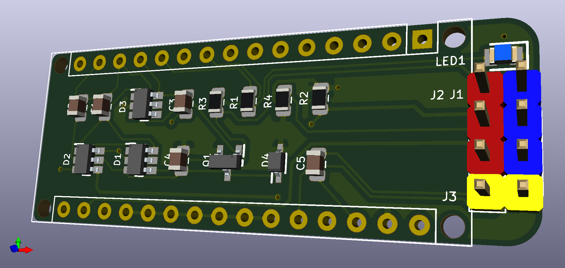
In this diagram, it is not clear where to connect tinyAVR? Can you add it (tinyAVR) to the diagram? https://raw.githubusercontent.com/wiki/Dlloydev/jtag2updi/images/NanoProgSch.png https://oshpark.com/shared_projects/cxgBKsCQ