Closed carstenpoulsen closed 3 years ago
Thx Carsten - it is possible to attach a zip file to the comments. The pads for the capacitors look small, what kind of capacitors do you use? They should withstand the maximum voltage you will apply, which can be up to 50 V or 100 V or more. I took 275V AC capacitors to be on the safe side.
Your welcome.
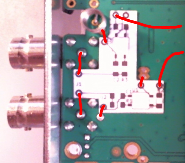
If you like the design, I will attach a zip when design is ready. The idea is to hot glue the PCB as indicated ion the picture. I have modified slightly: There is only one return path from pins 2 (already indicated as there is no red line from the topmost right pad)
I understand your concerns about the capacitor, but I have some experience in circuit designs with SMD. I have designed with C1206C104KARECAUTO which is rated to 250VDC. Sufficient for this application. https://api.kemet.com/component-edge/download/datasheet/C1206C104KARECAUTO.pdf
I am about to order 5pcs prototye PCB's The idea is to offer other interested for the cost. Maybe assembled. 10$+shipment
Sorry, but can I just connect probe via 100n capacitor (for example) instead of doing this all?
Sure you can. I think that you can buy DC-blockers in BNC connectors, so just do that.
The advantage of controlling from the menu is the opportunity to document what you do or have done. When you take automation a step further any feature that con be programmed and documented is an advantage.
I consider it an advantage to be able to easily flip between DC and AC coupling to assess both the DC and AC components of a signal.
Hello Carsten, nice PCB, I have only one concern about the small trace distance in the lower left (I'm automotive Q manager :) ), if you swap the J1 and J2 connections you will get a much more relaxed layout:
Hi Martin. Thanks for your nice words :-)
Well, yes. I could swap as J1 and J2 has equal value in the functionality. The distance between the J2-track and R1-pad has no electrical significance: 1: The spark-gap is sufficient as the signal DC component is assumed to be far less than 250V. Track/pad clearance is .35mm and the solder mask will add to isolation. 2: The track to pad capacity will merely add to the DC-blocking capacity.
So from a functional perspective I think the layout is fine.
If the track is moved closer to CH1 it may increase cross-talk. I am already concerned about the J2/J5 placement but decided that the overall pad placement was close to optimal concerning the wires to the topside and connections to input BNC's.
Let me know why you think your suggestion will relax the layout.
It's only my gut feeling, to paraphrase Goethe: Two souls dwell, alas! in my breast. As automotive guy I'm thinking in production lots of 10^6, ppm and strict layout rules, and in my former live I was responsible for building automation with direct connection to the mains (Cat III and Cat IV) and minimal creepage distances of 8 mm - solder mask was not accepted as reliable insulation. But this risk does not happen in our case and if the lightning strikes we are in trouble anyway.
P.S.: Also high capacitance KEMET capacitors are tricky - especially the low-voltage types that lose up to 30..40% of their nominal capacitance if working close to their nominal voltage - BTDT. But also this is not relevant for your application.
Drop a comment when you're happy with your development an I will announce this on the github project page and also in the user manual.
Your comments are highly appreciated. And relevant as review input.
When talking about 10^6 and strict rules we are in a different ball game. In that case the design and design process would be completely different.
I think PCB ver 1 is in en route in Germany. I will let you know.
@carstenpoulsen Any progress?
Hi Martin
Yes and no.
I made a mistake on the PCB so there is a new set smoking from China.
I assume a week or two, but I got the primary PCB layout verified and I’ve got the components so – soon.
/Carsten
From: Martin [mailto:notifications@github.com] Sent: 6. september 2020 15:08 To: OpenHantek/OpenHantek6022 OpenHantek6022@noreply.github.com Cc: Carsten Bøgh Poulsen carsten@boeghpoulsen.dk; Mention mention@noreply.github.com Subject: Re: [OpenHantek/OpenHantek6022] AC PCB (#109)
@carstenpoulsen https://github.com/carstenpoulsen Any progress?
— You are receiving this because you were mentioned. Reply to this email directly, view it on GitHub https://github.com/OpenHantek/OpenHantek6022/issues/109#issuecomment-687785046 , or unsubscribe https://github.com/notifications/unsubscribe-auth/ACCI5B6XCJVX6PNKE5DCVADSEOCR3ANCNFSM4PGUHNNQ . https://github.com/notifications/beacon/ACCI5B4EBPFI2QKO5IOSC7TSEOCR3A5CNFSM4PGUHNN2YY3PNVWWK3TUL52HS4DFVREXG43VMVBW63LNMVXHJKTDN5WW2ZLOORPWSZGOFD7MIVQ.gif
I have some assembled PCB's if someone is interested. I ship worldwide.
New PCB layout, modified for better wiring.
@carstenpoulsen I have just finished modifying my 3D printer so that it can etch PCBs. Would love the gerbers or whatever raw format you used. Even design files would be great. Will make for a nice little project to burn in the new mods to the printer.
@Ho-Ro Have you done any testing on how this mod may affect signals at the high end of the scopes capabilities? Concerned that the impedance mismatch caused by making could cause some sort of attenuation through reflections. Maybe even the max freq is too low for that though...
the impedance mismatch
I do not see any matched impedance, everything is in the high kΩ range while the copper traces are in middle Ω range. The max frequency is < 24 MHz (Nyquist), more than 10 MHz doesn't give a usable picture, so everything is fine. This scope is useful for (e.g. audio) measurements with steady signals and slow logic. Don't expect a tool for high speed logic, a cheap EzUSB LA with sigrok is better suited for this.
I was thinking for higher frequency signals where the scope probe would start to look more like it's characteristic impedance but of course with signals this low in freq it is not relevant. Still keen on those PCB design files so that I can etch something out...
@carstenpoulsen Any feedback on those gerbers that you offered in the opening post?
I don't think I offered gerbers as free issued items.
@carstenpoulsen
Right, I clearly misunderstood. Nothing a few minutes in KiCAD can't fix. I'll post the resulting files here once I'm done for all to benefit from in the sprit of this project and all other open source projects, if interested.
I'll post the resulting files here once I'm done for all to benefit from in the sprit of this project and all other open source projects, if interested.
@looxonline Nice, any open source contribution to this project is highly appreciated!
I'll post the resulting files here once I'm done for all to benefit from in the sprit of this project and all other open source projects, if interested.
@looxonline Nice, any open source contribution to this project is highly appreciated!
Almost got the PCB fabrication method 100% refined. As soon as I have absolutely consistent results the next step will be to push this board out.
Oh, that's beautiful! I'd definitely be interested in gerbers (or just pdf's so that I can etch my own).
I have a 6022BL which has a slightly different motherboard, but I think think your PCB's should still work OK. The big difference is that there are no convenient points on the PCB to access PE0 and PE3, so I'll have to solder them directly to the pins on the FX2
As this is not a real issue I will close now.
Easier AC installation I can provide a PCB layout if it has any interest. Please tell how to contribute this.