RandomHacks-Git / Best-Improvement-STM32

Source code for my Best Improvement board to control Best BST-863 hot air station
MIT License
5 stars 3 forks source link

stm32f103 - a few minor questions and feedback / 1st impressions #1

Closed dreamcat4 closed 3 years ago

dreamcat4 commented 3 years ago

Hi there, I am very pleased with this upgrade kit. And grateful for it. My prayers answered. However i did notice a few things inspecting the PCB. And just wanted to let you know. In case you decide to make revisions or updates for future runs.

Most of these are minor small points. Nothing really too important. So please don't take it as any criticism - you have done an excellent work. And with all the most important aspect really well done.

You can see here is a numbered list, for each point.

questions-feedback-annotated

  1. Is there any use here for RTC battery? Is it meant for having a clock or something? Are settings not need RTC, but instead they stored and remembered in the flash - yes? ...Because if there is no need for it at all, then I can instead cut the trace. And re-use those same terminal points for jumping to some other pins. With a mod wire. Please confirm if it does not matter.
  2. When soldering this GND pad, it was more difficult. Because of course the ground plane. However maybe if you make some cut out (gap) around the GND pad... then that will thermally isolate enough for an easier soldering experience. This is good for example here the LCD screen does not draw much current, so the ground connection is not so critical. It not matter (for me). But maybe some new user or person with a bad soldering iron. Then you can help them not to struggle so much.
  3. Here I can see you break out all the unused GPIOs - great! very good. However in the middle of this header you put the only breakout for the SWD debugging / programmer IO (SWD_CLK and SWDIO). This is not so good to take here (for SWD debug). Because there is no GND or +3v3 nearby. And no NRST pin. So what you want to do is keep it there. But also add dedicated separate SWD debug port. And include the other useful pins next to them. Perhaps something like this: [ 0v, SWD_CLK, SWDIO, 3v3, NRST ]. Or however you want to include them.
  4. This is NRST, ok no problem. I checked with DMM
  5. Buzzer polarity: I was not so sure which way around to install it. However reading online it seems to depend on the device whether polarity matter (or not). But I did check and got higher voltage from one side, which I guess means it has more space to move on the top side... it does not matter for me. I don't mind at all. Just thought to mention it. As perhaps it can make the buzzer sound louder (or more quiet). By reversing the polarity. Which is useful, to the preference. Of course there are also other easy ways to make it quiet. So no problem
  6. What are these for?
  7. Here is BOOT0. It is also useful for programming. However I could not find the trace, or know if the leg is broken out to any pin. I think this is good idea to make a pad for. In case we need to do programming for the open firmware. Typically you just make a 3 pin jumper, [ 3v3, BOOT0, GND ]. To pull it high or low (while flashing). Otherwise it floats internally

So that is all I can see here for suggestions to improve the PCB.

Programming / Debugging

Actually you did a really great job for the firmware. I do not plan to change very much. Except maybe if I require more than 3 presets. Then perhaps the buttons can be changed to scroll through numbered list of presets. Up, down, and select. Instead of directly switching to the preset.

However I will not add this until I really know that I need to keep more than 3 presets. So perhaps it won't be needed, then I will not add this.

And of course, as you also mention in your video: it is great to use the GPIO header, for connecting another slave device to control. For example fume extractor on/off. Or for attaching another input device, such as a foot switch pedal(s). So that hands are free. Thank you so much my friend!

RandomHacks-Git commented 3 years ago

WOW, thanks for the feedback. Let's see if I can answer your points, let me know if I miss anything.

1- I'm not using the RTC for anything and it might not even make sense to have this broken out but I thought someone could find a use for it. All the settings are indeed stored to flash so a battery is not required, this would only be used for time keeping and for this you would need to solder a 32.768kHz crystal and the respective load capacitors (Y1, C9, C10). To answer your question, yes you can cut the traces and use for something else but all unused (and some used, USB) pins are already broken out to the EXP header.

2- I didn't have this issue while soldering, the pad actually has thermal reliefs, I might have to check this as you make a good point with with the cheaper soldering irons. I actually widened the pads for the JST's and the THT resistors for the RP2040 version as they turned out quite small on this board. To be honest I don't know if I will continue to offer the kits, it turns out it takes a lot more time to put all the kits together than to actually solder everything.

3- I actually never program this with the SWDIO and SWCLK pins, I initially flash the bootloader with the TX and RX pins and then I just use USB to upload the firmware. I will take this into consideration in the next revision.

5- Yes, I forgot to edit the footprint's silkscreen, that + should not be there, as this is a passive buzzer the polarity should not matter, it only changes the direction the piezo element bends to, I didn't notice any volume difference on the boards I soldered. I already fixed this for the RP2040 version.

6/7- These are BOOT 0 and BOOT 1 they are set with a solder jumper but if you want to tinker with the board you can remove the solder and solder pins and use those tiny header jumpers 😉

For my daily use 3 presets are enough, I use one for heatshrink one for normal rework and one for higher temps, for anything else I just use the pots. You have some nice ideas I'm eager to see some hacks on my board hehe

dreamcat4 commented 3 years ago

Hello again! And thanks for these detailed replies. Very good

Here below explained is a very important point about 6/7. Thanks so much for explaining what those B0 and B1 were indeed connected to the boot0 pin an the boot1 pin.

This is the place where I needed to know how to change something, in order to get SWD working. Otherwise SWD does not connect (no response from target).

For some reason ST decided for a logic truth table, that having BOTH these pins set LOW (=GND)... then it breaks SWD. And it won't connect. This you have bridged on these inital batch of units by default BOTH to GND before shipping. Perhaps is might be something which you later on decide change for future units going forwards. Don't worry it's really simple to fix.

So here is my own direct findings from this evening;

boot0 boot1 swd best one?
0 0 fail
0 1 works <-- this
1 0 works
1 1 works

And here is the clue, which I found on the internet, somewhere on ST community forum (probably just taken from datasheet)

https://community.st.com/sfc/servlet.shepherd/version/renditionDownload?rendition=THUMB720BY480&versionId=0680X000006qMLd&operationContext=CHATTER&contentId=05T0X00000NPHqG&page=0

As you can see (rather not-helpful). But the behaviour for 0,0 is undefined. Which is silly they should know better! but heh :)


So why bother to go to all this trouble to make sure that SWD is working? Well to answer that...

In particular there are certain technical reason(s) why to now strongly prefer to use SWD protocol for both flashing and debugging. The a big reason primarily is convenience in PIO developer environment, where SWD interface allows the IDE to automatically flash, then reboot the chip. Then also automatically connect to the serial monitor (just like the arduino serial monitor). Which is to say... this is better than USB HID flashing protocol (which is broken).

Meybe you find rx/tx serial flashing just as easy (like arduino). However then you cannot do in situ hardware debugging. (with 0 effort, it's all over same cable). And also it occupies those 2 tx/rx pins.... well swd also is only 2 pins protocol. So you free up the serial port. And the USB port too. With SWD you can still debug them like (as is over separate dedicated link), while they are in use. It does not occupy them / block for running your application, or require rebooting into different 'fashing mode' etc. :+1:


So with this minor change I can now connect over SWD (using OpenOCD program, in linux). And dump the existing flash to back it up (in case I brick my device later on). And this then lets me try flashing myself. Not had time to play with yet. Just took a dump to finally report a successful connection. Is working! Very pleased / happy with this situation.

Here is the command I used to connect after pullint b1 = HIGH. This commant is for taio TUMPA v2 programmer. So to be clear: you will need a somewhat different cmdline to connect using other programmer model, such as the very popular STLINK v2. You will need to specify different config .cfg file to load. So that openocd program can know how to talk to other model of programmer device. But that configuration part is just to establish the connection. It does not affect the communication over telnet, to send the commands sent on the SWD link.

openocd -s tcl -f interface/ftdi/tumpa.cfg -f interface/ftdi/swd-resistor-hack.cfg -c "transport select swd" -f target/stm32f1x.cfg -c "reset_config srst_only connect_assert_srst"

Open On-Chip Debugger 0.10.0+dev-01266-gd8ac0086-dirty (2020-05-27-14:47)
Licensed under GNU GPL v2
For bug reports, read
    http://openocd.org/doc/doxygen/bugs.html
none separate

Info : FTDI SWD mode enabled
Warn : Transport "swd" was already selected
swd
srst_only separate srst_nogate srst_push_pull connect_assert_srst

Info : Listening on port 6666 for tcl connections
Info : Listening on port 4444 for telnet connections
Info : clock speed 1000 kHz
Info : SWD DPIDR 0x1ba01477
Info : stm32f1x.cpu: hardware has 6 breakpoints, 4 watchpoints
Info : stm32f1x.cpu: external reset detected
Info : starting gdb server for stm32f1x.cpu on 3333
Info : Listening on port 3333 for gdb connections

then you open up a 2nd terminal window, and telnet into the running openocd server:

telnet localhost 4444
Trying 127.0.0.1...
Connected to localhost.
Escape character is '^]'.
Open On-Chip Debugger
> flash list
{name stm32f1x base 134217728 size 0 bus_width 0 chip_width 0}
> flash read_bank 0 boot01.bin
device id = 0x20036410
flash size = 64kbytes
wrote 65536 bytes to file boot01.bin from flash bank 0 at offset 0x00000000 in 0.908111s (70.476 KiB/s)

also you can query the chip for it's memory may layout too,

> dap info
AP ID register 0x14770011
    Type is MEM-AP AHB3
MEM-AP BASE 0xe00ff003
    Valid ROM table present
        Component base address 0xe00ff000
        Peripheral ID 0x00000a0410
        Designer is 0x0a0, STMicroelectronics
        Part is 0x410, Unrecognized 
        Component class is 0x1, ROM table
        MEMTYPE system memory present on bus
    ROMTABLE[0x0] = 0xfff0f003
        Component base address 0xe000e000
        Peripheral ID 0x04001bb000
        Designer is 0x4bb, ARM Ltd.
        Part is 0x0, Cortex-M3 SCS (System Control Space)
        Component class is 0xe, Generic IP component
    ROMTABLE[0x4] = 0xfff02003
        Component base address 0xe0001000
        Peripheral ID 0x04001bb002
        Designer is 0x4bb, ARM Ltd.
        Part is 0x2, Cortex-M3 DWT (Data Watchpoint and Trace)
        Component class is 0xe, Generic IP component
    ROMTABLE[0x8] = 0xfff03003
        Component base address 0xe0002000
        Peripheral ID 0x04000bb003
        Designer is 0x4bb, ARM Ltd.
        Part is 0x3, Cortex-M3 FPB (Flash Patch and Breakpoint)
        Component class is 0xe, Generic IP component
    ROMTABLE[0xc] = 0xfff01003
        Component base address 0xe0000000
        Peripheral ID 0x04001bb001
        Designer is 0x4bb, ARM Ltd.
        Part is 0x1, Cortex-M3 ITM (Instrumentation Trace Module)
        Component class is 0xe, Generic IP component
    ROMTABLE[0x10] = 0xfff41003
        Component base address 0xe0040000
        Peripheral ID 0x04001bb923
        Designer is 0x4bb, ARM Ltd.
        Part is 0x923, Cortex-M3 TPIU (Trace Port Interface Unit)
        Component class is 0x9, CoreSight component
        Type is 0x11, Trace Sink, Port
    ROMTABLE[0x14] = 0xfff42002
        Component not present
    ROMTABLE[0x18] = 0x0
        End of ROM table
$ md5sum boot01.bin 
9f481217d0d13ab66bafd720a921072b  boot01.bin

$ hexdump boot01.bin | head -20
0000000 2800 2000 00f1 0800 0139 0800 0139 0800
0000010 0139 0800 0139 0800 0139 0800 0000 0000
0000020 0000 0000 0000 0000 0000 0000 0139 0800
0000030 0139 0800 0000 0000 0139 0800 0139 0800
0000040 0139 0800 0139 0800 0139 0800 0139 0800
*
0000090 04f9 0800 0139 0800 0139 0800 0139 0800
00000a0 0139 0800 0139 0800 0139 0800 0139 0800
*
00000e0 0139 0800 0139 0800 0139 0800 f85f f108
00000f0 2100 f000 b804 4b0b 585b 5043 3104 480a
0000100 4b0a 1842 429a f4ff aff6 4a09 f000 b803
0000110 2300 f842 3b04 4b07 429a f4ff aff9 f000
0000120 fa45 4770 1918 0800 0000 2000 02c8 2000
0000130 02c8 2000 030c 2000 f7ff bffe 4770 4770
0000140 4770 2803 bf8c 2002 2000 4770 4770 0000
0000150 4b03 681b 7a9b b113 4b02 2205 601a 4770
0000160 0304 2000 0310 2000 4770 4770 4770 4770
0000170 4770 4770 4b01 2204 601a 4770 0310 2000
0000180 b510 f000 fc77 4b21 4a21 681b 2400 6812

next time, I shall try compiling, flashing etc. in vscode. Using platformIO ide. However 1st I must convert your project into a PIO directory layout. And rename / move the source code files about. For example: main.INO ---> src/main.cpp

Looking forwards to this :)

dreamcat4 commented 3 years ago

Hi again. Just forgot to mention, if ever adding a dedicated SWD port...

This is just only a suggestion, because there is no standard, and is different pinout on official ST discovery boards. However most people get the 'blue pill' or the 'black pill', and they have this header:

stm32 Blue pill:

blue pill - swd programming port

stm32 Black pill:

black-pill - swd programming port

RandomHacks-Git commented 3 years ago

Great work. I can definitely ship the boards with BOOT 1 set high, I usually set BOOT 0 high and BOOT 1 low to upload the bootloader over tx/rx and then just move BOOT 0 to low (and upload the firmware over USB as this way I also make sure the USB is working correctly) but as long as everything works as it should it's no problem for me to set BOOT 1 high too.

Moving to platformio is something I'm looking to do for a loooong time as arduino IDE is way behind, I always say to myself "this is the last project I'm going to do on arduino ide" but when I'm in the mood to program (which to be honest doesn't happen often) I always end up opening arduino ide as I can start right away and it doesn't require me to watch a tutorial to figure out how everything works like setting the board and what not, hope I finally switch over on the next project 😅

Your suggestions are much appreciated 👍

dreamcat4 commented 3 years ago

Sure man! Hey if you inevitably get stuck in any places with switching over PIO then don't be afraid to ask for some assistance. You can email me (dreamcat4 at gmail) with the problem. And will try my best to get you past such stuck point.

But am not so familiar with windows specific problem (being on linux). For example installing python on windows, or openOCD on windows. But they should probably do those part in the official vscode extensions / installers

dreamcat4 commented 3 years ago

OK so here is now the same command, but modified for the more popular STLINK v2 programmer:

openocd -d4 -f interface/stlink.cfg -c "transport select hla_swd" -f target/stm32f1x.cfg -c "reset_config srst_only connect_assert_srst"

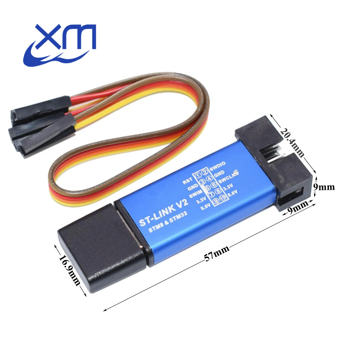
This is the recommended device for SWD connection within platform io environment. Here is an example of the STLINK v2 looks like,

https://www.aliexpress.com/item/32792513237.html

RandomHacks-Git commented 3 years ago

Hey, sorry for the late reply. I do have an STLink v2, used it before to flash a tv set top box. I just noticed that setting BOOT1 high actually breaks the USB communication so I can't ship the boards like this.

dreamcat4 commented 3 years ago

sure man no problem. what i would suggest here is to install jumper headers, instead of solder bridges. and also more clear label that these are for boot0 and boot1 pins. not to confuse people thinkink its gpios port b0 and b1.

the other thing we can do is improve here the markdown Readme documentation here with annotated images and arrows / comments. (or as a wiki if you prefer instead)

actually i have now a few photos which is suitable for that purpose. just have not gotten around to organising it properly. my priority has instead been tweaking the source code. to compile in PIO / vscode. which is coming soon will be uploaded to my fork

RandomHacks-Git commented 3 years ago

Yes next batch of PCBs will have a better label for the boot pins. Most people are probably never going to change the state of the boot pins so I don't think I will solder the extra headers and include the jumper but, who knows, maybe in the future.

I want to write a small instructions manual with all the information but I haven't had much time as I'm working on several projects simultaneously.

dreamcat4 commented 3 years ago

Huh, it's not known to me, for why initial connection failed over SWD, with both boot0 and boot1 set to GND. Perhaps it's something to do with this device (f103 chip), or otherwise the maple bootloader. You see I have only used before the 'black pill' with simultaneous serial + SWD both running together. And black pill is newer stm32f4xx series. With more features and new HAL / IO subsystem.

Anyway, today I did the following things:

Next will reassemble the whole unit. And check it's working and operating as normal. To know that the new firmware build is all works the same as before. For example that the exact library dependencies were chosen correct.

Also I noticed and can confirm the arduino serial device /dev/ttyACM0, it does not appear unless I have set the both boot0 and boot1 back to GND. So I have now done that after the re-flashing. In order to check display on the serial port.

BTW why is serial output disabled by default in the options? Is there some negative effect on the performance, or something else that it causes a problem?

RandomHacks-Git commented 3 years ago

What's new on 102? Once again since most people won't use the serial output I do not see the need to ship the boards with it enabled, the serial prints will of course increase the loop time but shouldn't have any significant effect on performance. Serial can be enabled/disabled by a long press of any of the two arrow keys and the state is saved to flash.

dreamcat4 commented 3 years ago

Sorry I did not make myself clear enough....

The reason i want the serial output is to check the firmware is functioning after flashing. Same for the firmware version to check there is new version been flashed. It's just for my own testing purpose here.

The thing is that getting a connection from the computer with USB serial is also dodgy. Because the length of the USB cables, and difficulty powering the board etc.

Anyhow I have just reassembled everything. And it does generally seem to be working, except for the display. Which is completely black.

This may be some issue with my device.... or it could be an issue with the LCD display library, which is chosen by the library dependancies of PIO. Or perhaps it could be some other issue with the code migration. IDK

However I have kind of run out of time to look into it further. What I need to do is reflash the original firmware image, and see if the display works. To rule out hardware issue. Then after that investigate the source code a bit more. Or Visa versa (both ways).

But while I have run out of time here. Meantime you can see / browse the code changes on my new branch. To look at what I have been doing to get it to compile in platformIO environment. (and it also includes you last changes for the farenheight steps)

https://github.com/dreamcat4/Best-Improvement/commits/feature/convert_to_platform_io

Good day

RandomHacks-Git commented 3 years ago

So are you not using serial over USB?

You can power the entire board with USB without any issues if you bridge the two pads next to the micro USB connector or you can power the board over the jst connector that connects to the motor controller board and still use USB (make sure the bridge is open if you power it this way). The solder jumper is open by default so there is no backfeed of the 5v to the computer and this way you can turn the station off even if you keep it connected to a powered USB. The rp2040 version will have a diode footprint instead of the solder bridge, I might also add a 2 pin header footprint so it is easier to enable/disable usb power if needed.

About the display, I test all the boards before shipping so I doubt it is an hardware issue with my board but let me know if you can't get it working. Is the backlight on?

Nice I will have a look at your code.

dreamcat4 commented 3 years ago

Uh yeah i guess i could power it with the ESC connector, +15v dc from my bench PSU. That would make more sense, than trying to power over USB. Because usb power is not so great here (for me, with these cables I have). So will leave the bridge open

Yes, the backlight comes on, however the LCD itself is all black. Crystals are twisted. No i do not think your PCB is the reason. It's more likely other issue for example the LCD library, maple framework etc.

The other issue I forgot to say was the heater is not coming on. Actually I was concerned maybe if the previous guy destroyed the heater element (because the fan was broken, not coming on to be cooling the heater enough). However just now I measure 49.7 ohms between the heater -+ terminals. Which seems normal i guess we will get there eventually.

First must look into the LCD display

dreamcat4 commented 3 years ago

@RandomHacks-Git ok so...

if you remember i had some connection issues with the programmer. This turned out to be bad swclk and swdio lines on my programmer cable. One of the header pins was only half engaged (the little 'click' in the plastric plug). And also these data and clock lines were twisted together. which is bad because it creates cross-talk, between those lines.

After noticing and fixing the cable. Then have flashed back the original firmware backup (from 1st earlier dump in openocd).... that was all easy afterwards. Also did have to move the jumper boot1, and return it back again after flashing. So that the firmware would boot. And then was OK working back again

=====

My display hardware, with your upgrade board installed. It all functions OK, the LCD display works great. This means the LCD display issue (black screen). It exists somewhere in the PIO firmware build, or in the upstream LCD library. For those code changes I made let us see now....

Can you please confirm... Is this the correct version of the LCD library to use? Or should it be different library here>

https://github.com/dreamcat4/Best-Improvement/blob/feature/convert_to_platform_io/platformio.ini#L40

I had some minor small fixes to get it to work under linux, But nothing important was changed. Here:

https://github.com/dreamcat4/HT1621/commits/master

It's based on the last commit was hash commit 1ca058d2d677b130cba23216641073719817effd

https://github.com/dreamcat4/HT1621/commit/1ca058d2d677b130cba23216641073719817effd

If this is not the problem... then maybe the problem is some place elsewhere. For example in the Maple library... so while you check this. Then I will keep looking. Many thanks

RandomHacks-Git commented 3 years ago

Hi, yes that is the library I used, I didn't modify anything so it should work.
What CPU frequency are you using? I use 72MHz, not sure if a different frequency could affect the SPI timings and break communication. (also make sure there are 5v on the board either by powering it with USB or the ESC connector as the lcd needs 5v to work) Is the rest of the code running? Have you checked if it isn't stuck somewhere?

dreamcat4 commented 3 years ago

Well that took a long time... Other things to do got in the way.

After coming back find out my STLINKv2 dongle stopped working. No longer respond with target. Ordered 2 more from China which doesn't arrive yet.

Had to spend another 1-2 day to figure out how to make debugging work with my other programmer. That nobody else has (TIAO TUMPA v2). Got it working just now! Awesome

So what the place where have got is that I can step over the setup() and can see the point where the backlight is turned on/off. However the backlight... is NOT controlled over the LCD spi bus, right? Which is not the problem. Backlight seems to work just fine no problem.

So then setup() gets into the LCD library to init. And there is this bit to check it can respond valid data. Well I uncommented and enable these 2 lines and step into it in the debugger

https://github.com/dreamcat4/HT1621/blob/master/ht1621.cpp#L27-L28

However data returned back is different than was written. And the check fails. But IDK if that is a valid test. Because in many situation we do not typically need to hear anything back from an LCD any return messages. Because it's purely an output device. So that might just not matter IDK

Anyhow I also check which GPIO pins is configured for the LCD. It is as you published in the public code here for the LCD. Which is this bit:

https://github.com/dreamcat4/Best-Improvement/blob/feature/convert_to_platform_io/src/main.cpp#L83

And like... the library uses standard feature DIGITAL_WRITE to signal the pins for the spi bus. Which I guess we would not normally expect to have any issue.

In my platformio.ini file did uncomment the cpu clock freqency to be 72Mhz too. As you mentioned that could be a problem...

https://github.com/dreamcat4/Best-Improvement/blob/feature/convert_to_platform_io/platformio.ini#L37

However that did not change anything. Issue still occur.

This is where I am now. Maybe I need to bring out the logic analyzer and debug the communication between the MCU and the LCD

Being able to step through in the debuger is helpful. Actually maybe I can stop execution when it's doing the writes to the GPIO pins. And probe them. Without needing to get out the logic analyzer. We chall see! Interesting! ;)

dreamcat4 commented 3 years ago

ok so as far as i can see... the wr pin is the clock pin to wite data to the lcd. And it latches in the what is put onto data line, onto the shared bus. And that is the line which is not working here:

Screenshot from 2021-08-05 10-29-35

so i checked for the continuity etc. for the connection to the logic analyzer was ok. seems was not any bad connection

Looking at the code the wr line is PA15 (pin 38 on the physical package). Is declared in the code as integer enum 25. But maybe then it adds an extra offset to get the real pin number IDK

But this seems like the issue. Because other communication pins looks working. Also this result agrees with the previous testing / checking, whereby the contents stored memory location read back / returned back is different than was written

Will need to dig deeper. And see what stops the pin PA15 from working

dreamcat4 commented 3 years ago

ok have some more information, about this issues around driving the LCD here...

what i did was to add some extra lines at the beginning of setup(). to manually step through in the debugger. and set each of the 4 digital pins as OUTPUT mode. And then digitalwrite() each one in turn, first to logic LOW, and then back to logic HIGH

when probing with DMM, what was discovered was each line starts as +5v. because it's being pulled up by the LCD driver IC. then they all (except for PA15, which is broken here) go to 0v (correct), but then setting high it goes back to +3.3v instead of +5v

So this is because the LCD library here initializes the pinMode() to OUTPUT

https://github.com/dreamcat4/HT1621/blob/master/ht1621.cpp#L12-L15

however the correct pinMode setting should be OUTPUT_OPEN_DRAIN. Because that is how to pul low muti voltage (5v <--> 3v3) and is safer way. To avoid uncertain voltage levels.

But that is not the issue, we know (because it already works to drive the LCD). So what about the PA15 pin?

Well measuring this pin, it reads 4.04v constant on the DMM. Which is werid. However that might be the multimeter averaging the value, of some higher frequency. That it cannot see properly. Same for the logic analyzer IDK.

Anyway have just found this, it seems like the reason here:

https://www.stm32duino.com/viewtopic.php?t=70

Because it's shared as a JTAG pin (JTDI). So this is disabling the usage as GPIO. For this SWD debugging. And using SWD for flashing too.

So that also makes me wonder if also other JTAG pins you have used... might also be disabled. Because another thing I noticed was no heating. So maybe for the heater GPIO pin, is also blocked by the JTAG too

What I am not so sure for now... what to do about this. Because on one hand they say to disable + enable programming ports. To release the JTAG only pins. But it might risk loosing SWD capability. Since you did not break out NRST to have the RESET signal to MCU. I think you shuold break out NRST in this case on the programing header. As an optional usage when needed.

The other solution is for me to find some other unused GPIO pin. Cut existing track. Then run a small mod wire(s), from alternate GPIO pins. And that might be better or worse solution IDK

But at least we find some reasons now. And more exactly to recommend for your next PCB revision. If you want the live debugging feature over SWD protocol.

dreamcat4 commented 3 years ago

@RandomHacks-Git ok, the problem is fixed now in the PIO git branch:

https://github.com/dreamcat4/Best-Improvement/commit/f099b5816d17b0e1f0f905189a33b49f524a8e5d

the LCD works now. however i still have to do some more testing on this branch. to make sure everything else works (like the heater GPIO pin for example). and reinstall it back together into the case

dreamcat4 commented 3 years ago

I also find out something else. When the LCD is plugged in. Then it creates unwanted interference on the SWD data lines. And the debugger cannot attach. The SWD programmer reports data transmission error, while the reset button is held down.

If i remove the LCD module from the main PCB. Then the SWD connection is successfully established. But not otherwise. This is with both the boot pins set to 0.

So maybe the changing of the boot pin configuration has some connection to the interference coming from the LCD module. Do you have an oscilloscope? Because unfortunately I do not have here. For observing the crosstalk on the data lines etc.

What does this mean? Well it makes this PCB more difficult to debug. Because the SWD connection is unreliable. This could be impoved in a future PCB revision. Along with adding NRST. At least the good news is there is not conflict with the setting for the boot0,1 pins. Which is a good news.

At this point I'm just going stop messing about. And reinstall the PCB back into the machine. To test all functions on the [re]build. Make sure it works

RandomHacks-Git commented 3 years ago

Nice troubleshooting. So in the end did you change PA15 to another GPIO or did you get it working as is?

The only LCD trace that intersects the SWD/SWC traces (on the other layer of the board of course) is the data pin (PB9) and the traces are at 90 degrees to each other creating the smallest intersection area possible so I'm not sure if crosstalk is the issue you are having, but it certainly is possible, I do have an oscilloscope but my time is very very limited right now unfortunately.

I will take note of all the suggestions you made so far so I can take them into consideration if I ever design another stm32 revision 😉

dreamcat4 commented 3 years ago

yeah the fix was just to add +1 line in at the beginning of setup() routine. which is call enableDebugPorts(); in the git code commited, already linked above ^^. and now the dispaly works. everything working. no need to use any different GPIO for that one.

and i must say, having just tested the features now. it's my first time ever to get this station working. since before was broken (the blower fan). and it's really impressive. the usability is really awesome. and having the P mode (potentiometer mode) gives a 4th preset. It's so nice to use a real pleasure. Was well worth it, the extra time to get it working. Thank you so much again

So for the interference problem on SWD (coming from the LCD daughter board). IDK what is actually causing this. But maybe a simple solution is to make a jumper bridge on the 2 power pins that supply +5v power to the LCD module (and also the touch too). So that it can be powered off independantly while programming. By removing a jumper link. Just like with these boot pins, by default the jumper is soldered across. To be always on. But then the user can remove it, or install a manual switch to power off the whole LCD module. This then should stop all interference disruption on the SWD programmer lines. If it is not a cross-talk, then maybe it is spikes on the GND line instead IDK

Yes there is no hurry to look into any of those issue. It's mostly to document and keep a record here for later on. And to make sure that the new code branch for Platform IO is compiling, and working same as original code. Which I have flashed tested now today. And is confirmed to work

Lastly am cleaning up the platformio.ini file a bit. Which includes all of the project settings for building and flashing etc. I upload tonight to the branch

dreamcat4 commented 3 years ago

OK great, I am closing this issue. This work is now concluded. And also have other things to do, like use this fabulous hot air station!

However if in the future anytime you ever need to come back here to ask for further clarification about anything specific. Then please don't hesitate. Happy to help if i can remember what was about.

And good luck with your struggles! For changing the MCU etc. and other challenges. I hope you are successful. Certainly I am already recommending this station / mods to all my friends now. Mot that they can get it! hehe. Certainly I feel very fortunate to have gotten this rev1 board while it was available. Thank you so much it's really works so amazingly well. A great pleasure to use this station now

dreamcat4 commented 3 years ago

Again back here recording this extra solution, for posterity (to know it, remember it). There is nothing concerning not to worry about it. Is just a small hardware bug in my own unit:

With the final step to put back the last metal cover. Something strange happen, that the unit does not power up correct reliably anymore. Either nothing happen, or the fan comes on. But with no display. Or the display flash briefly and then switch off.

Then I remove the cover, and still not booting. But then I want to check that your mainboard is receiving a clean +15v power rail. Once the front power switch is put ON position.

So jabbing the multimeter probes into +15v + GND (on the ESC board header, where the +15v comes from)... it magically boot and starts working again. I replace the cover, it happen again. Same thing

However in fail state, the +15v rail reads something like +2v only. (or that is the PSU capacitor, which is not fully drained). I am guessing that for some strange reason there is not enough current draw taken by your new mainboard. Is too effecient. Or maybe I somehow degrade or the PSU on my ESC board. From previous hot air rework (to replace the fan driver). Whatever the reason IDK

However simply adding a 120k ohm resistor between +15v rail and GND. On the header cable. Now it boots much more reliably. Every time. So I am also wondering now... if that can help too... for the previous issue I encounter here. That the SWD link is disrupted when the LCD is plugged in. Because of a junk noise / data returned back while the MCU is held in reset state.

I do not want to go back now and try this. Because am finished for the time being. However it's just simply noted to remember for later. Next time. Since to have the LCD plugged in is the fully assembled state. And makes future debugging much easier. Not to have to dismantle everything. And be blind without the display connected.

Of maybe some other simple type of a filter caps etc. If not on the +15v power rail. Then instead on the +5v rail, or 3v3. Or closer to those SWD programmer lines IDK. Something to look at for next time