Closed CoreRasurae closed 2 years ago
In general, you should not generate clocks using logic; such clocks aren't guaranteed to work either in simulation (due to simulation semantics not being defined for such clocks) or in synthesis (due to LUTs not being glitchless on most FPGAs). See also #625.
Thanks for your reply. Still I have two additional questions and comment...
According to Peter Alfke of Xilinx Applications in this post: https://groups.google.com/g/comp.arch.fpga/c/F6AYhYzDmi0?pli=1 It is stated that: "Here is what I wrote ten years ago ( you can find it, among other places, in the 1994 data book, page 9-5:
Function Generator Avoids Glitches ... Note that there can never be a decoding glitch when only one select input changes. Even a non-overlapping decoder cannot generate a glitch problem, since the node capacitance would retain the previous logic level... When more than one input changes 'simultaneously', the user should analyze the logic output for any intermediate code. If any such code produces a different result, the user must assume that such a glitch might occur, and must make the system design immune to it... If none of the address codes contained in the "simultaneously" changing inputs produces a different output, the user can be sure that there will be no glitch....
This still applies today."
Comment: According to the above there should be no glitch at least in the LUT output for the case where the clock signal is ANDed or ORed with the CSn signal, since they aren't simultaneously changing in reality. In the SPI protocol the SPI clock must be stable before CSn goes low or high. In the real application the only clock condition that needs to be added to the LUT is:
m.d.comb += clkSPIDom.clk.eq(spiClkPin.i | csnPin.i)
So there are no glitches in reality,
Question 1: Given this limitation how does one simulate a clock signal that isn't always active? Like the SPI clock? In this case, this is only required for the simulation case, because in real applications there would be no need to add logic to the clock signal, since the clock is already generated that way.
Question 2: If I understand correctly the Amaranth FSM does not allow asynchronous reset. How could I insert an asynchronous reset to the FSM? Or should I emulate a FSM with a switch statement that would allow asynchronously resetting to the initial state? This could provide a workaround for part of the simulation.
Note that there can never be a decoding glitch when only one select input changes. Even a non-overlapping decoder cannot generate a glitch problem, since the node capacitance would retain the previous logic level
This doesn't match my understanding of the current technology. That said, I will make no strong claims here--I haven't put in nearly enough time researching this issue to do so. In any case, that's the less important part.
When more than one input changes 'simultaneously', the user should analyze the logic output for any intermediate code.
Amaranth, and the FPGA-specific toolchain it feeds input to, generally make no guarantees about the synthesis results. It's certainly possible to translate logic to glitchless LUTs, but none of the components specifically attempt to do so. It may happen that the LUTs generated for your logic are glitchless for any particular input and toolchain versions, but I wouldn't recommend relying on that, since it's not a part of the toolchain contract.
You could, of course, instantiate the LUTs directly (with the keep
attribute, or its equivalent for your toolchain, to avoid them being optimized). That's not much different from instantiating a clock gating primitive.
Given this limitation how does one simulate a clock signal that isn't always active?
I suggest using a simulator process to generate the clock.
How could I insert an asynchronous reset to the FSM?
An Amaranth FSM can be placed in a clock domain with asynchronous reset. This is the same as any other logic; other than instantiating primitives directly, you can't get a register with an asynchronous reset either.
Thanks for your reply.
I was indeed able to simulate the dummy protocol by generating the clock signal using a simulator process that also exhibits the behavior of the combinatorial logic that has to be inserted in the real device. The simulation results with the clock generated this way are indeed consistent. This solution can be found in the attached SimpleFSMSolution1.zip
The other alternate way for achieving consistent simulation results was to also generate the clock using a simulator process and enabling asynchronous reset for clock domain to which the FSM is attached. This solution can be found in the attached SimpleFSMSolution2.zip
Both solutions work properly and simulate properly. From my side this issue is now clarified and can be closed.
When I was implementing a slave Quad SPI controller with amaranth I found two cases, one where the simulation indicates that the device will work, but in reality it does not, and another where in simulation it indicates that device will not work, but in reality it works. I have simplified the project and created a simplified serial controller with a FSM that is able to reproduce the issue. (Example can be found in the attachment along with examples of the two issues)
Issue 1: The simulation indicates that the device will work, but in reality it does not. This is the scenario in the attached example SimpleFSMClient1. In this case the simulation clock is set to be:
that is, the serial clock signal is only generated during the data transmission, when the CSn (negated Chip Select) signal is active. In this case, in reality, the FSM misses one extra clock cycle to come out of the FSM
Data
state into theIdle
state, thus failing to make it ready for receiving a second transfer. However in simulation despite the needed and missing extra clock cycle the simulation says it will come toIdle
state at the end of transfer, whenserialCSn
signal goes high/inactive. This simulation result is generated when the signals between the modules are set like so:The result can be seen here:
Issue 2: The simulation indicates that the device will not work, but in reality it does work. This is the scenario in the attached example SimpleFSMClient2. In this case the simulation clock is set to be:
that is, the serial clock is generated only when
serialCSn
when signal is low/active and an extra clock cycle is generated by theserialCSn
signal itself. Here thesimpleFSMClient2.simpleFSM.fsmState != 0
condition is not required in reality, but only for simulation, because serialCSn starts low by default, despite the simulation process setting it high as early as it can. The condition ensures that the extra cycle is only generated when the FSM machine has its current state set to a nonIdle
state.This scenario was tested with a Xilinx XC7S15 (Spartan-7) and is working properly in the device. The simulation however indicates that the FSM machine will get stuck in the
Data
state, thus failing the second transfer. This simulation result is caused when the followingserialCSn
signal assignment is used:as depicted here:
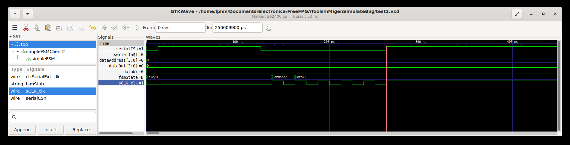
In summary:
serialCSn
is assigned with:serialCSn
is assigned with:Data
state at the end of the first transferIdle
state at the end of the first transferSimpleFSM.txt SimpleFSMClient1.txt SimpleFSMClient2.txt