Open kdojeteri opened 5 years ago
That is exactly how I have the FET soldered, so I am not sure what is causing your issue. You can try desoldering the FET and bridging the bottom left (source) and right (drain) pad - here is the pinout. This should bypass the reverse polarity protection and allow you to power the module directly. Make sure you only apply the 3.3V.
You can also try some continuity checking. In a reverse polarity protection circuit with an n-channel FET, the negative of the battery should be connected to the drain, the ground of the circuit (GND pin on module) should be connected to the source and the gate should be connected to both the positive terminal of the battery and the VCC pin on the module.
Thanks for the tip. I will try bridging the pads. Jut a quick question: Do I have to have the battery connected in order to connect the programmer?
No, leave the battery disconnected and power it via the 3.3V on the programmer. The pinout of the header from bottom to top is:
Bridging the pads made it so that the programmer's indicator (the blue LED) would stay on. Before, it would turn of the moment I connected GND and VDD. But with the bridged FET pads, as you suggested, I still couldn't connect to the chip via OCD.
Open On-Chip Debugger 0.10.0
Licensed under GNU GPL v2
For bug reports, read
http://openocd.org/doc/doxygen/bugs.html
Info : The selected transport took over low-level target control. The results might differ compared to plain JTAG/SWD
adapter speed: 1000 kHz
Info : Unable to match requested speed 1000 kHz, using 950 kHz
Info : clock speed 950 kHz
Info : STLINK v2 JTAG v17 API v2 SWIM v4 VID 0x0483 PID 0x3748
Info : using stlink api v2
Info : Target voltage: 3.211556
Error: init mode failed (unable to connect to the target)
in procedure 'init'
in procedure 'ocd_bouncer'
In a desperate attempt involving lots of continuity checking and misinterpreting the results, I left the FET pads unconnected. Strapping the programmer to the board in this state (no FET, no bridge, nothing) allowed OpenOCD to connect, or at least that's what I thought. When I tried flashing it, it failed.
Open On-Chip Debugger 0.10.0
Licensed under GNU GPL v2
For bug reports, read
http://openocd.org/doc/doxygen/bugs.html
Info : The selected transport took over low-level target control. The results might differ compared to plain JTAG/SWD
adapter speed: 1000 kHz
Info : Unable to match requested speed 1000 kHz, using 950 kHz
Info : clock speed 950 kHz
Info : STLINK v2 JTAG v17 API v2 SWIM v4 VID 0x0483 PID 0x3748
Info : using stlink api v2
Info : Target voltage: 3.200525
Info : nrf51.cpu: hardware has 4 breakpoints, 2 watchpoints
Info : accepting 'telnet' connection on tcp/4444
target halted due to debug-request, current mode: Thread
xPSR: 0xc1000000 pc: 0xfffffffe msp: 0xfffffffc
Warn : Unknown device (HWID 0x000000d1)
Error: Failed to enable read-only operation
Error: Failed to erase reg: 0x4001e508 val: 0x00000000
Error: Failed to erase sector @ 0x00000000
Error: Failed to write to nrf51 flash
Error: error writing to flash at address 0x00000000 at offset 0x00000000
Info : dropped 'telnet' connection
Error: jtag status contains invalid mode value - communication failure
Polling target nrf51.cpu failed, trying to reexamine
Examination failed, GDB will be halted. Polling again in 100ms
Info : Previous state query failed, trying to reconnect
Polling target nrf51.cpu failed, trying to reexamine
Info : nrf51.cpu: hardware has 4 breakpoints, 2 watchpoints
As a sanity check, I soldered the same chip to a spare mitosis receiver board and tried programming it there. That completed successfully. So the chips aren't bad. It must be something about the boards or how I soldered them.
no FET, no bridge, nothing
In this case there is no path to ground and there should be no continuity between the NRF51 GND pin and the GND pin on the programming header. I am surprised you managed to power up and connect to the NRF module in this state. Can you please check continuity between the GND pin on the header and the GND pin of the NRF51 (without the programmer connected)?
Other than that, there should be nothing wrong with PCB, especially when you short out the GND and GND_P pads on the "top" side of the board (NRF module is on the bottom).
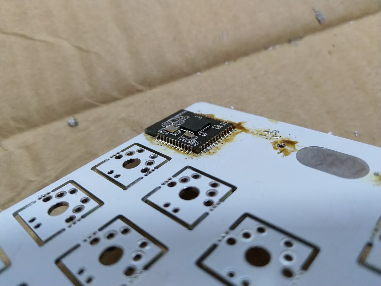
CONTENT WARNING: copious amounts of rosin in pics below First of all, thanks for making this keyboard available. It's been an amazing, albeit very long journey getting all parts and fitting everything together.
However I got stuck trying to program the keyboard PCBs. Whenever I try to connect my ST-Link V2 to the header, it just shuts off as if it had come across a short or something.
Now I have practically no knowledge of electronics, but I have tested for shorts between all the header pins and there isn't one. I then tried to test for continuity between header ground and Yj-14015 module ground, I got some voltage drop, but still continuity. I suspect the voltage drop is due to the transistor and is normal.
Speaking of, you moved the FET slightly as opposed to Mitosis, which raises my doubts about whether I soldered it on the right side. Could you check my photos? Could you please also check for anything I might've missed that could cause my programmer to freak out?
All photos are of the to-be right half of the keyboard:
For right angle headers I instead used straight headers and connected them via a solder bridge