Open HuyKhac opened 6 years ago
Hi @HuyKhac , Sorry for late reply. I've tested with your code on the latest master with following log print:
ESP_LOG_BUFFER_HEX(TAG, reg_data, 4);
for (int i = 0; i< 4; i++) {
printf("%d, %d\n", reg_data[i]&0x40, reg_data[i]&0x4);
}
When I connect GPIO 22 to VCC, it shows:
I (286) test: cc cc cc cc
64, 4
64, 4
64, 4
64, 4
While below if connect GPIO 22 to GND:
I (286) test: 88 88 88 88
0, 0
0, 0
0, 0
0, 0
This means in some way the QIO mode can reads from DAT2 correctly. The reason is possibly:
I've no your commit ID, neither your slave spec. And your return data length (BBAA, 16 bits) doesn't match your total length on the snapshot (4x8bits). So I cannot tell whether it's which reason. Please try the ways above, and if you still have problem, please comback with more information (slave spec, actual reg_data value (4bytes), commit id).
Hi @ginkgm,
Thanks for your reply. 1-About ESP IDF, my version was not the latest. I will try again after updating my IDF 2-About my logic analyzer setting, it is Saleae logic analyzer, and I dont see it has threshold level setting. Actually, I captured a waveform of another MCU platform running the same scenario and it shows the same response waveform from the slave device and that MCU can read back data correctly. 3- About your suspect on clock edge at data output, it is positive edge to capture data. My slave device is FT813 from FTDI. 4-About my return length of 16-bit value, as I said, the driver code reads 4 bytes (4x8bit) then returns 2 last bytes as the valid data. You can see in my print log, it has "I (2183) GPU: Rd16=aa,0,aa,bb" which prints out 4 bytes at Rx phase.
In short, I will re-run the code with latest IDF and update you soon.
HuyK
Hi @ginkgm,
I updated IDF to the latest commit 03d78e7 and retry. Before changing to QSPI mode, I pre-write the register at addr 0x3020c0 to value 0xFFEE, then read back to confirm (it can read back 0xFFEE correctly). Then I change to QSPI mode and try to read back that register, it still gives wrong read value although the waveform is correct. Here is the print log:
VC1 register ID after wake up 7c
I (1103) FT8XX: Before: 0xffee
I (1103) FT8XX: Switch to QSPI
I (1103) GPU: Re-init SPI into QSPI
I (1103) FT8XX: Try to read in QSPI mode
I (1103) GPU: Rx:0xee,0x0,0x0,0x0
I (1103) FT8XX: After: 0x0
E (1113) FT8XX: QSPI read fail[0 - 400]
I (1113) FT8XX: Init done
It prints "Before: 0xffee" for the first read back in single SPI mode It prints received raw 4 bytes in QSPI mode "GPU: Rx:0xee,0x0,0x0,0x0" It prints proceeded read value: "After: 0x0"
Here is the function to read register data:
uint16_t Ft_Gpu_Hal_Rd16(Ft_Gpu_Hal_Context_t *host, uint32_t addr)
{
uint16_t value;
uint8_t spiData[4] = { 0 };
Ft_Gpu_Hal_StartTransfer(host, FT_GPU_READ, addr); //to assert CS and send out reg addr
spi_readn(SPIM, spiData, host->spinumdummy + 2); //reading phase
if(print_data)
{
ESP_LOGI(TAG, "Rx:0x%x,0x%x,0x%x,0x%x",spiData[0],spiData[1],spiData[2],spiData[3]);
}
value = spiData[host->spinumdummy] | (spiData[host->spinumdummy + 1] << 8);
Ft_Gpu_Hal_EndTransfer(host); //deassert CS
return value;
}
Note: host->spinumdummy = 2 (it expects to use last two bytes from raw RX data)
Here is the function to read SPI:
static void spi_readn(spi_device_handle_t spi, uint8_t* data, uint16_t len)
{
spi_transaction_t trans;
memset(&trans, 0, sizeof(trans)); // Zero out the transaction
trans.length = len * 8; // transaction length is in bits.
trans.tx_buffer = NULL; // no TX Data
trans.rx_buffer = data; // Rx buffer
trans.rxlength = trans.length;
if(Current_SPI_Mode == QSPI_MODE)
{
trans.flags |= SPI_TRANS_MODE_QIO;
}
spi_device_transmit(spi, &trans);
}
What could be wrong here?
Thanks HuyK
Hi @HuyKhac , Still can't reproduce your issue, data are read correctly from my side (commit d099ff125, not far from yours). Maybe there's conflicts on your bus, since the . I found this: https://www.corelis.com/education/tutorials/spi-tutorial/
Please check:
I also confirmed that when I use QIO to read, the lines will be freed as soon as the first posedge of reading clock (so dummy bits are really required). After that, external devices are able to take control of the bus in the becoming 8 clocks.
Hi @ginkgm ,
For you questions:
About CS signal Yes, it is inactive after a writing and I keep it active before the address fields and until the last data bit. You can view the flow of Ft_Gpu_Hal_Rd16(). And I can confirm CS waveform is correct.
About the dummy bits I do not understand what you mean. But from the waveform, I see ESP32 output reg addr correctly and the slave device drives I0-I3 in reading phase correctly. Can you guide me more about the dummy bits? How to configure and check it?
I will try to use another USB scope (PicoScope 2000) because I dont have a big oscilloscope here.
On SPI bus, there are ESP32 and FT813 devices, no other devices share the bus.
Thanks for the support to work on this issue.
HuyK
Ok, I think I understand the dummy bits. Actually, in the code, at reading phase, it already provides clocks to read 4 bytes which counts for 2 dummy bytes and then 2 valid data bytes. So I think my application code already handles dummy bits insertion on the bus. Am I correct?
Can you try to add 10KR pullups on 4 data lines?
I see this from the tutorial
"Figure 8 shows an example read command for a Spansion S25FL016K serial NOR flash device. To read from the device, a fast read command (EBh) is first sent by the master on the first IO line while all others are tristated. Next, the host sends the address; since the interface now has 4 bidirectional data lines, it can utilize these to send a complete 24-bit address along with 8 mode bits in just 8 clock cycles. The address is then followed with 2 dummy bytes (4 clock cycles) to allow the device additional time to set up the initial address."
I see it talks about 2 dummy bytes (4 clock cycles). Why do you see a dummy byte as 8 clocks?
If you are confirmed that your device respond corretly, maybe you can try to add 10kR pullups on 4 data lines.
Yes I can confirm the slave device can output data in QSPI correctly, because when I tried to change the pre-written value different than 0xFFEE to that register, the output waveform is changed accordingly. I will try with pullup register on 4 data lines
I will post more waveforms to show cases when it reads different values of that register and overall CS active/inactive.
Hi @HuyKhac , Could you please help me do this test to see whether it fix your issue?
#include "soc/gpio_sig_map.h"
#include "soc/io_mux_reg.h"
#include "soc/gpio_struct.h"
void gpio_matrix_in(uint32_t gpio, uint32_t signal_idx)
{
//don't bypass gpio matrix
GPIO.func_in_sel_cfg[signal_idx].sig_in_sel = 1;
PIN_INPUT_ENABLE(GPIO_PIN_MUX_REG[gpio]);
}
gpio_matrix_in( GPIO_NUM_19, VSPIQ_IN_IDX);
gpio_matrix_in( GPIO_NUM_23, VSPID_IN_IDX);
gpio_matrix_in( GPIO_NUM_22, VSPIWP_IN_IDX);
gpio_matrix_in( GPIO_NUM_21, VSPIHD_IN_IDX);
Thanks @ginkgm, I will try all suggestions and update you soon
Hi @ginkgm,
Here is my update to you: 1- Add calling to function gpio_matrix_in() after re-init to QSPI mode The result is unchanged 2-Then add 10K pull-up resistors to 4 data lines The result is unchanged 3-Try to probe with Digilent Discovery2 scope and get same waveforms
Lets me add more info about the code, basically, it will init VSPI in Single SPI mode and do initialization to FT813 chip. After initialization, it will re-init VSPI to QSPI mode for high-speed data transfer when in operation. I post all main functions to work with VSPI here for complete information to you.
This is the function to init VSPI in single SPI mode:
ft_bool_t Ft_Gpu_Hal_Open(Ft_Gpu_Hal_Context_t *host)
{
esp_err_t ret;
/* Setup to SPI mode */
spi_device_handle_t spi;
spi_bus_config_t buscfg={
.miso_io_num = FT_SPI_MISO,
.mosi_io_num = FT_SPI_MOSI,
.sclk_io_num = FT_SPI_SCK,
.quadwp_io_num = -1,
.quadhd_io_num = -1,
};
spi_device_interface_config_t devcfg={
.clock_speed_hz = FT_FREQ_HZ,
.spics_io_num = -1,
.queue_size = 7, //We want to be able to queue 7 transactions at a time
.command_bits = 0,
.address_bits = 0,
};
//Initialize the SPI bus
ret = spi_bus_initialize(FT_SPI_HOST, &buscfg, 1);
if(ret != ESP_OK)
{
ESP_LOGE(TAG, "Failed to add SPI device");
return false;
}
ret=spi_bus_add_device(FT_SPI_HOST, &devcfg, &SPIM);
if(ret != ESP_OK)
{
ESP_LOGE(TAG, "Failed to add SPI device");
return false;
}
/* Configure a IO for FT CS pin */
gpio_config_t io_conf = {
.intr_type = GPIO_PIN_INTR_DISABLE,
.mode = GPIO_MODE_OUTPUT,
.pin_bit_mask = 1LL << host->hal_config.spi_cs_pin_no,
};
ret = gpio_config(&io_conf);
if(ret != ESP_OK)
{
ESP_LOGE(TAG, "Failed to add CS pin");
return FALSE;
}
gpio_set_level(host->hal_config.spi_cs_pin_no, 1);
/* Configure IO for LCD CS pin */
gpio_set_direction(PIN_NUM_LCD_CS,GPIO_MODE_OUTPUT); //LCD CSX
gpio_set_level(PIN_NUM_LCD_CS, 1);
/* Configure an Expanded IO for PD pin */
gpio_config_t io_conf1 = {
.intr_type = GPIO_PIN_INTR_DISABLE,
.mode = GPIO_MODE_OUTPUT,
.pin_bit_mask = 1LL << GPIO_NUM_17,
};
ret = gpio_config(&io_conf1);
if(ret != ESP_OK)
{
ESP_LOGE(TAG, "Failed to add CS pin");
return FALSE;
}
gpio_set_level(GPIO_NUM_17, 1);
gpio_config_t io_conf2 = {
.intr_type = GPIO_PIN_INTR_DISABLE,
.mode = GPIO_MODE_OUTPUT,
.pin_bit_mask = 1LL << GPIO_NUM_16,
};
ret = gpio_config(&io_conf2);
gpio_set_level(GPIO_NUM_16, 0);
/* Initialize the context valriables */
host->ft_cmd_fifo_wp = host->ft_dl_buff_wp = 0;
host->spinumdummy = 1;//by default ft800/801/810/811 goes with single dummy byte for read
host->spichannel = 0;
host->status = FT_GPU_HAL_OPENED;
Current_SPI_Mode = SPI_MODE;
return TRUE;
}
This is the function to switch to QSPI mode:
static void gpio_matrix_in(uint32_t gpio, uint32_t signal_idx)
{
GPIO.func_in_sel_cfg[signal_idx].sig_in_sel = 1;
PIN_INPUT_ENABLE(GPIO_PIN_MUX_REG[gpio]);
}
ft_int16_t Ft_Gpu_Hal_SetSPI(Ft_Gpu_Hal_Context_t *host,FT_GPU_SPI_NUMCHANNELS_T numchnls,FT_GPU_SPI_NUMDUMMYBYTES numdummy)
{
ft_uint8_t writebyte = 0;
/* error check */
if((numchnls > FT_GPU_SPI_QUAD_CHANNEL) || (numdummy > FT_GPU_SPI_TWODUMMY) || (numdummy < FT_GPU_SPI_ONEDUMMY))
{
return -1; //error
}
host->spichannel = numchnls;
writebyte = host->spichannel;
host->spinumdummy = numdummy;
if (FT_GPU_SPI_TWODUMMY == host->spinumdummy)
{
writebyte |= FT_SPI_TWO_DUMMY_BYTE;
}
Ft_Gpu_Hal_Wr8(host, REG_SPI_WIDTH, writebyte);
//Check to re-init ESP32' SPI in Half Duplex device so that we can transfer in QSPI mode
if(numchnls == FT_GPU_SPI_QUAD_CHANNEL)
{
//host->ft_cmd_fifo_wp = Ft_Gpu_Hal_Rd16(host, REG_CMD_WRITE);
ESP_LOGI(TAG, "Re-init SPI into QSPI");
spi_bus_remove_device(SPIM);
spi_bus_free(FT_SPI_HOST);
esp_err_t ret;
/* Setup to QSPI mode */
spi_device_handle_t spi;
spi_bus_config_t buscfg={
.miso_io_num = FT_QSPI_IO1,
.mosi_io_num = FT_QSPI_IO0,
.sclk_io_num = FT_SPI_SCK,
.quadwp_io_num = FT_QSPI_IO2,
.quadhd_io_num = FT_QSPI_IO3,
.max_transfer_sz= 16*320*2+8
};
spi_device_interface_config_t devcfg={
.clock_speed_hz = FT_FREQ_HZ,
.mode = 0,
.spics_io_num = -1,
.queue_size = 7, //We want to be able to queue 7 transactions at a time
.flags= SPI_DEVICE_HALFDUPLEX,
};
//Initialize the SPI bus
ret = spi_bus_initialize(FT_SPI_HOST, &buscfg, 1);
if(ret != ESP_OK)
{
ESP_LOGE(TAG, "Failed to add QSPI device");
return false;
}
ret=spi_bus_add_device(FT_SPI_HOST, &devcfg, &SPIM);
if(ret != ESP_OK)
{
ESP_LOGE(TAG, "Failed to add QSPI device");
return false;
}
gpio_matrix_in(FT_QSPI_IO1,VSPIQ_IN_IDX);
gpio_matrix_in(FT_QSPI_IO0,VSPID_IN_IDX);
gpio_matrix_in(FT_QSPI_IO2,VSPIWP_IN_IDX);
gpio_matrix_in(FT_QSPI_IO3,VSPIHD_IN_IDX);
Current_SPI_Mode = QSPI_MODE;
}
return 0;
}
Here is definition for IO pins:
#define FT_FREQ_HZ (1*1000*1000)
#define FT_QSPI_IO0 GPIO_NUM_23
#define FT_QSPI_IO1 GPIO_NUM_19
#define FT_QSPI_IO2 GPIO_NUM_22
#define FT_QSPI_IO3 GPIO_NUM_21
#define FT_SPI_MOSI GPIO_NUM_23
#define FT_SPI_MISO GPIO_NUM_19
#define FT_SPI_SCK GPIO_NUM_18
#define FT_SPI_CS GPIO_NUM_5
#define FT_SPI_HOST VSPI_HOST
Here are functions to read data from FT813:
ft_uint16_t Ft_Gpu_Hal_Rd16(Ft_Gpu_Hal_Context_t *host, ft_uint32_t addr)
{
ft_uint16_t value;
ft_uint8_t spiData[4] = { 0 };
Ft_Gpu_Hal_StartTransfer(host, FT_GPU_READ, addr);
spi_readn(SPIM, spiData, host->spinumdummy + 2);
if(print_data)
{
ESP_LOGI(TAG, "Rx:0x%x,0x%x,0x%x,0x%x",spiData[0],spiData[1],spiData[2],spiData[3]);
}
value = spiData[host->spinumdummy] | (spiData[host->spinumdummy + 1] << 8);
Ft_Gpu_Hal_EndTransfer(host);
return value;
}
ft_void_t Ft_Gpu_Hal_StartTransfer(Ft_Gpu_Hal_Context_t *host,FT_GPU_TRANSFERDIR_T rw,ft_uint32_t addr)
{
if (FT_GPU_READ == rw)
{
ft_uint8_t spidata[4];
spidata[0] = (addr >> 16);
spidata[1] = (addr >> 8);
spidata[2] = addr & 0xff;
if(Current_SPI_Mode == QSPI_MODE)
{
gpio_set_level(GPIO_NUM_16, 1);
}
spi_open(SPIM, host->hal_config.spi_cs_pin_no);
if(Current_SPI_Mode == QSPI_MODE)
{
gpio_set_level(GPIO_NUM_16, 0);
}
spi_writen(SPIM, spidata, 3);
host->status = FT_GPU_HAL_READING;
}
else
{
ft_uint8_t spidata[4];
spidata[0] = (0x80 | (addr >> 16));
spidata[1] = (addr >> 8);
spidata[2] = addr;
spi_open(SPIM, host->hal_config.spi_cs_pin_no);
spi_writen(SPIM, spidata, 3);
host->status = FT_GPU_HAL_WRITING;
}
}
ft_void_t Ft_Gpu_Hal_EndTransfer(Ft_Gpu_Hal_Context_t *host)
{
spi_close(SPIM, host->hal_config.spi_cs_pin_no);
host->status = FT_GPU_HAL_OPENED;
}
static void spi_open(spi_device_handle_t spi, int cs_pin)
{
gpio_set_level(cs_pin, 0); //active CS pin
}
static void spi_close(spi_device_handle_t spi, int cs_pin)
{
gpio_set_level(cs_pin, 1); //in-active CS pin
}
static void spi_writen(spi_device_handle_t spi, const uint8_t* data, uint16_t len)
{
uint32_t tx_len;
spi_transaction_t trans;
memset(&trans, 0, sizeof(trans)); // Zero out the transaction
#define MAX_SPI_TRANSFER (4*1024-4)
do
{
if(len > MAX_SPI_TRANSFER) tx_len = MAX_SPI_TRANSFER;
else tx_len = len;
trans.tx_buffer = data; //point to user buffer for Tx data
trans.rxlength = 0;
trans.length = tx_len*8; //translate to length in bits
trans.flags = 0;
trans.rx_buffer = NULL;
if(Current_SPI_Mode == QSPI_MODE)
{
trans.flags |= SPI_TRANS_MODE_QIO;
gpio_set_level(GPIO_NUM_16, 1);
}
esp_err_t ret = spi_device_transmit(spi, &trans);
if(ret != ESP_OK)
{
ESP_LOGE(TAG, "Failed to Tx");
}
data += tx_len;
len -= tx_len;
}while(len);
gpio_set_level(GPIO_NUM_16, 0);
}
static void spi_readn(spi_device_handle_t spi, uint8_t* data, uint16_t len)
{
spi_transaction_t trans;
memset(&trans, 0, sizeof(trans)); // Zero out the transaction
trans.length = len * 8; // transaction length is in bits.
trans.tx_buffer = NULL; // TX Data
trans.rx_buffer = data; // Rx buffer
trans.rxlength = trans.length;
if(Current_SPI_Mode == QSPI_MODE)
{
trans.flags |= SPI_TRANS_MODE_QIO;
}
spi_device_transmit(spi, &trans);
}
So it will call Ft_Gpu_Hal_Open() to init single SPI and send some settings to FT813. Then it calls Ft_Gpu_Hal_SetSPI() to switch to QSPI; next it will call Ft_Gpu_Hal_Rd16() to read register data.
I attach different waveforms when it reading different pre-written values from the register. It shows that the slave device - FT813 - outputs correct data but ESP fails to read in
When the register has value 0xAB89:
Zoom-out to show CS sequence:
Zoom-in to show data signal lines
When the register has value 0x5A9D Zoom-out to show CS sequence: Zoom-in to show data signal lines
Summary:
Please help to review all my code in this post if I miss anything to make it work.
Thanks, HuyK
Hey
Hope this is not too much of a late reply.
In your function:
static void spi_readn(spi_device_handle_t spi, uint8_t* data, uint16_t len)
In half duplex mode, when you are reading, you need to ensure that:
trans.length = 0; // you are not writing anything in this phase of qspi
trans.rxlength = len * 8; // you are reading len * 8 bits
When in the writing phase you need to reverse them:
trans.length = len * 8; // you are writing len * 8 bits
trans.rxlength = 0; // you are not reading anything in this phase
Hope this helps.
Dom
Despite this being an old thread, I have the exact same problem. From this issue report (and other similar relating to half duplex) it seems like half duplex and DMA is just broken. I cannot get that data that shows in the scope to fill in the read buffer - it is just returns all zeros after the first byte, i.e. it reads and fill one byte but actively zeros all others. If I switch to full duplex mode then it works fine but I need half duplex so I can use dual/quad mode.
I have experienced the same results as this (#4456) and other issue reports. The data lines probed with oscilloscope report the awaited bits, but the read buffer does not fill correctly.
Environment
Problem Description
I try to use VSPI in QSPI mode to increase communication speed. ESP32 can write out register address, but when it reads back register data, IO2 bit is always read as 0 although it is 1 in a probed waveform. Here is my code to configure VSPI in QSPI mode:
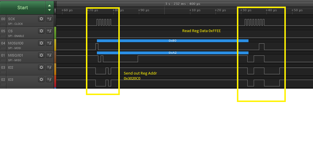
The register addr is 0x3020C0 and the expected register data is 0xFFEE. However, ESP32 reads back as 0xBBAA ( all IO2 bits are read as 0). If IO2 bits are read as 1 then, it will return 0xFFEE which is expected. I capture the waveform to check, IO2 bits are correctly output by slave device, but ESP32 always read as 0s.
I attach the waveform here. Note that in reading reg data phase, it reads 4 bytes but uses last 2 bytes (that requirement comes from the slave device.
Here is the print log from ESP32 showing that it reads back reg data as 0xBBAA
Should I miss anything? Is there any bugs in SPI driver in QSPI mode?
This is the waveform I captured for that the test. It shows correct waveform sent from the slave device
Thanks, Huy