jharvey / Charge_Controller

MPPT hardware which uses FUGU firmware
17 stars 2 forks source link

Design review #1

Open krzysztof9nowak opened 2 years ago

krzysztof9nowak commented 2 years ago

Hi, I am no electronics guru, but here are my suggestions.

Schematic:

jharvey commented 2 years ago

Hmmm, fuses are to prevent fire. Typically located at the source so you remove the source of energy. I typically don't size fuse to protect the devices, I typically size to protect the wires or things that can catch fire. I also don't like fuses, it's hard to properly size them for I2T issues. In this case the pulsing will cause high amps for short periods of time, so I2T issues are elevated. I tend to think the fuse should be closer to the panel, if it should be there at all. Some times I use a fuse as it's easier to repair then a burnt copper trace.

L1 includes Digikey part number 495-5076-ND. The schematic properties includes part numbers for either JLC or Digikey. I was planning for 12AWG wire, and I used this prediction tool to predict 6 wraps. https://coil32.net/online-calculators/ferrite-torroid-calculator.html I think 10AWG might also fit, but insulation thickness is likely a concern. Of course if you need more windings, then it may not work either.

I recently found the below. Any thoughts about cramming 50A through a SO8 package? https://jlcpcb.com/partdetail/MagnTek-MT9223CT50BR5/C2930869

I'm concerned about I2R on the traces. I included J33 and J34 as an option to add a copper wire to help keep the current off the PCB layers.

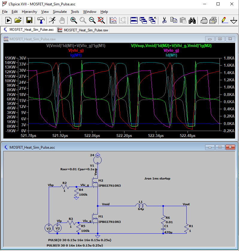
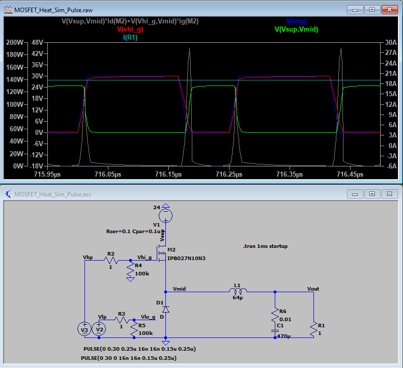
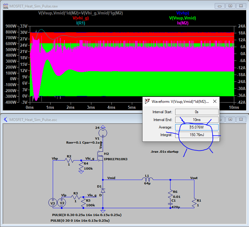
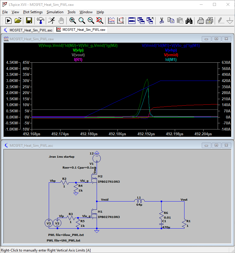
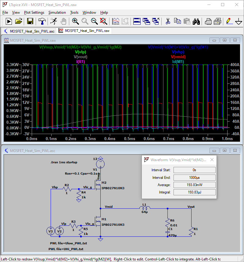
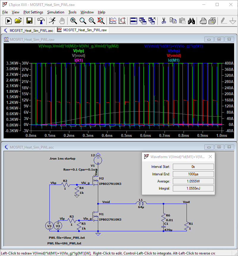
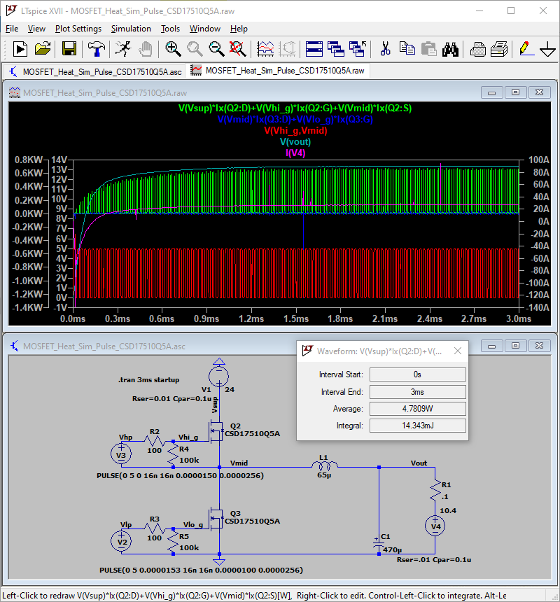
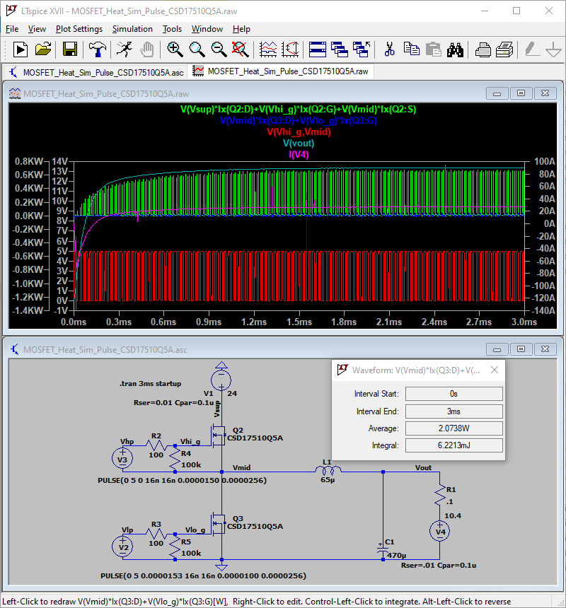
I was not able to make meaningful predictions of heat generated by Q1, Q2 or Q3. Rds generated watts was not helpful, the real heat will be the transient conditions. 2.6mOhm * 35A^2 = 3W. I don't much about what the losses will be during the switching. How many watts do we think we need to get out of these? Q3 also wants more electrical insulation from the heatsink. Which isn't going to help the situation. I also should pick a fan and some how include that in the 3D printed case. If I had some kind of prediction of the watts, or some kind of empirical data to work from, then I could make a better thermal prediction.

Q1 and Q2 secretly conduct a bunch of the electrical energy via the screw on the tab. I expect the copper layers are not large enough, but copper with tabs bolted together should be good. Looks like the C7 change will either be a huge layout change or I might just bolt the cap to heat sink. That's going to be a bit of work to change.

I hear you about the current loops. I'm expecting this to be around 20kHz. Is that a proper frequency to be expecting? I really don't know the low core frequency to be considering.

I'm USA eastern standard time. If a phone call helps perhaps we can phone.

jharvey commented 2 years ago

This is a good layout reference https://www.maximintegrated.com/en/design/technical-documents/tutorials/5/5450.html specifically the simulations showing you that at about 1KHz the ground plane currents start to follow the matching trace.

jharvey commented 2 years ago

I've tried several simulations to predict the heat generated by Q1, Q2, and Q3. So far this is the best I've managed. It uses a similar but different MOSFET and actually simulates without crashing. I see PSPICE for TI offers the actual MOSFET being used. However it appears the spice model has a typo in the .ENDS part of the SPICE model, as it errors out and does not compile. In the LTSpice I'm learning how to create an equation to multiple the instantaneous V * A for the MOSFET, then I can plot that to see the instantaneous watts.

Perhaps worth nothing, this simulation suggests the 100ohm series gate resistor is limiting pulse. I'm not sure if that would be the same in the real world or not. But it might warrant a close review.

image

jharvey commented 2 years ago

Small progress, looks like I'll have to use the pulse file power supply, which allows precision timing of the pulses. Currently this model shows KA and KW of energy dissipated by the MOSFET's. So Looks like I'll have to create a spreadsheet which will then create the timing pulses. This will allow precision timing of dead times. Anyhow incremental progress. image

jharvey commented 2 years ago

I wonder if I can get LTSpice to integrate so I can make a prediction of the heat generated by the MOSFET. In the below simulation, with only the high side drive, I see these large but short spikes of heat. Like 300W during the transition stage, and basically 0W any other time. I really need to know the area under the curve to know what kind of energy the heat sink needs to deal with.

image

jharvey commented 2 years ago

In LTSpice after you run the simulation, you can add probes. If you hit the alt button, then select a component, it will graph the instantaneous watts for that component. Then if you hit crtl and click the text of that trace, it will integrate what ever is in the graph. I did this for just the high side MOSFET, of similar Rds while it was running at about 19 amps. For 10mS it averaged at 15W.

image

jharvey commented 1 year ago

I've got the PWL file created and now the simulation seems a bit more sane. How does this look? I can now control the delays between the high and low sides. This zoomed in view shows the transient spikes in amps and watts.

image

For the high side I get a watts prediction in the low mW

image

For the low side I get a watts prediction around 1W. image

Do these predictions seem sane? I feel like the original design had a fan for a reason. With this particular pulse train, when the output is 5V @ 4A. Under those conditions I guess the heat sinks handling 1W is not that crazy. I guess I need to figure out how to get the pulse train to produce more volts and more amps.

jharvey commented 1 year ago

@krzysztof9nowak

  • The radiator seems a bit small, do you have any thermal specs or calculations for it?

The simulation has finally produced some results. I obtained the SPICE for the CSD17510Q5A from PSPICE for TI, by exporting the file, then importing it into LTSpice. This seems to be producing a fairly decent watts generated prediction.

It's not perfect, I couldn't get the simulation to always work, for some reason it would lock up if V1 went above about 31V, then it would start working again if it was at around 48V. I'm assuming that's some kind of limit embedded in the SPICE file. However if it was at around 48V, the MOSFET's claimed to dissipate KW instead of W, As well I had to be cautious when V4 was around 15V, as it would commonly back flow L1. With these limitations in mind, and with some very finely tuned on and off times, I think I have a fairly good prediction of the watts that Q2 and Q3 generate. I believe Q1 is just on or off, so the RDS predictions for that should be fine. So we'll call that 35A^2 * 3mOhm = 3.7W.

In the below, Q2 claims 27A output and less then 5W.
image

Then Q3 in this same simulation is 2W. image

I see many items which need to be very closely monitored. For example the V2 the parameter which is 0.0000153 needs to be between about 0.0000151 to 0.0000155. If it's outside that range, then the MOSFET dissipates KW instead of W.

For now I'll plan for Q2 = 5W and Q3 = 2W. So I'll call it about 10W total.

The MOSFET max junction temp is 175C, and it has 0.5C/W from junction to heatsink.

The HeatSink has a about 6C/W rise with a small fan, but could be 2.5C/W with a more powerful fan.

So rise is about 10W * (0.5C/W + 6C/W) = 65C rise. So the ambient could be as high as 110C before it hits the limit of the MOSFET junction. The ambient is more likely to be below 40C, so the rise could get up to 105C. I tend to start getting concerned above 85C, as FR4 often starts to fatigue around 85C. As well a 3D printed case is probably only good to around 45C to 55C.

I think the heatsink in the BOM should be OK, but I would prefer if it was larger. I'd prefer it if worked better with out a fan.

jharvey commented 1 year ago
  • What core are you using for L1? 6 turns seems to be low for 64uH.

During my simulations efforts I found the below. It's only 17.2A, but it's a purchasable option, and I don't have to design it's internals, they simply tell me it can handle 17.2A so I assume the saturation is OK up to 17.2A. https://octopart.com/search?q=7443783533650

jharvey commented 1 year ago

@krzysztof9nowak

I have published a revised design. Thank you for your feedback. If you feel so inclined a second review would be great. Here are some key notes of interest. -- L11 is the intended inductor, or you can optionally wind your own L1. L11 has a datasheet with published temperature rise, I'm a bit concerned about this expected rise in temp. -- 100x41x8mm Aluminum Heat Sink seem reasonably priced on ebay. HS1 could have a screw to keep a tight fit to this heat sink. The heat sink will need clearance for thru hold components. These clearance areas could be done with a hand drill. -- I left U2, as I don't see how to make this work with a bootstrap circuit. -- in higher power designs, J33 and J34 could bolt to a heatsink, which also helps keep the currents off the GND plane.

krzysztof9nowak commented 1 year ago

Hi, sorry for lack of response, I was busy with other work. I see you really played around with the simulations. As you observed the dead-time is critical, but thankfully that's handled by the IR2104 driver. Also thanks for the nice LTSpice tricks.

I think everything looks okay and you are good to go.

lekrom commented 1 year ago

Hi @jharvey,

Looks fairly good.

I do have a few comments:

  1. I like the idea using the ideal diode circuits as reverse polarity protection. The part number you assigned (LCSC) for the corresponding zeners (To limit Vgs) indicates 5.6V types. I recommend going up to the neighborhood of 10V in order to get the Rds(on) as low as you can go for the sake of efficiency. Also, with the ideal diodes in place, the BCCU should no longer be required and allows for quite a bit of simplification. Getting rid of the BCCU would offset some of the added losses due to the higher Rds(on) of the 2 PMOS FET's in the circuit. You could of course use NMOS FET's on the low side rails for the ideal diode implementation instead of the high side PMOS FET's, should reduce the losses even further.
  2. I do not understand the need for all the test pins around the ESP32, they are all connected to unused pins?
  3. You could move the ESP up a bit to have the antenna section flush with the board edge. A cutout on this edge around the antenna will also clear it whilst saving some real estate (and eliminate the need for the bulge in the enclosure).
  4. The fan connector seems way overkill.

-Regards, Lekrom

jbaltes commented 1 year ago

L1 part saturation: TDK 495-5076 allows 500mT at 25dgrC vor 410 at 100dgrC (Material N27): https://www.tdk-electronics.tdk.com/download/528850/3a7f957d754f899aec42cd946598c5c4/pdf-n27.pdf B=NIAL/Ae=610A1940nH/33.63mm^2=3461mT - so I think saturation is violated with this core even at only 10 A