 lucysrausch
commented
5 years ago
lucysrausch
commented
5 years ago Hey Niklas, thanks for your great suggestions and the time you spent on thoughts about this :)
1) I don't think an additional ground plate helps for this design. I think so for two reasons: First, GND of the bottom pcb is connected to the shielding of the USB type C cable, which is usually connected to an earthed computer or a laptop. For reference, I've experienced no difference in performance id I connected the ground cable of a scope probe. Second, I tried to avoid as much metal underneath the coil as possible, as it creates eddy currents. That's also the reason why I have a cutout in the middle of the pcb. I didn't mind that for the first revisions, and changing this made a huge difference. That is also the reason for the opto-coupler: I measure a voltage drop of 1.2V induced just from one side of the pcb to the other side. The opto-coupler helps isolating these domains.
2) That's a great hint, thanks! I did think about this before, but I never actually measured the actual voltage on the rail. The USBLC4LC6 does have an internal zener diode, but I don't know how well it performs.
Anyway, I wanted to try implementing primary current feedback for the next revision. This would also have the advantage that I can implement a phase lead circuit (google "DRSSTC phase lead") to compensate for the propagation time added by the deadtime logic. I was thinking of using a pcb-only current transformer as described here: http://sci-hub.tw/https://ieeexplore.ieee.org/document/7931056/ I wanted to do the next design in four layers anyway, so this might work out pretty well.
I also have some other ideas for this project. One of them is to implement a "QCW" mode by using the flyback transformer to ramp up the bridge voltage. I don't think this will work with USB, but with an external power supply this might give some pretty cool effects. Of you want to collaborate on this, feel free to keep giving suggestions :)
Best, Niklas
 nikisalli
Hi Niklas, i'm Niklas! :) i have quite a lot of experience from tesla coils i made in the past and sometimes i had the exact same problem with my coils. i think adding a ground plane on the bottom of the coil to make a better earthing system might help you to solve this issue and improve the overall stability of the system.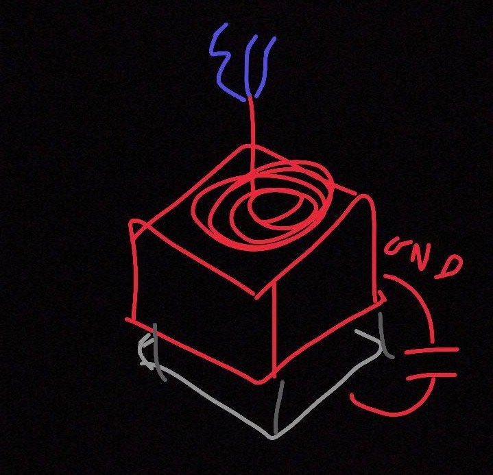 the capacitor should be around 100nF and rated for 200V or more. i do this in both big and small coils and usually it results in better stability of the feedback system.
another thing i thought of is that the diodes on the feedback system have not enough capacitors near them so when you touch the sparks and the current coming from the secondary coil increases it may cause a big ripple voltage on the 5V rail (maybe you could probe this with an oscilloscope).
a solution to this might be to completely isolate the feedback system from the secondary coil with a current transformer or an antenna (not suggested because usually makes things really unstable) or you could just add bigger bypass capacitors near the diodes and a capacitor and bigger resistor in series to the secondary coil like in the image below.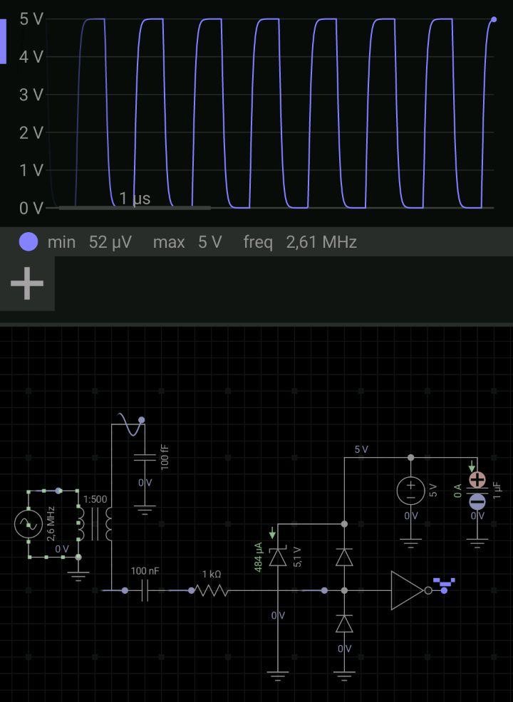 the 100 femto farad capacitor is a bit too low to simulate the resonant parasitic capacitance your coil creates i think but i used it to make a quick simulation at your coils' working frequency.
I hope you'll solve this in the next version of the coil ;)